


KiCad: How to draw a curved coplanar waveguide
Drawing a curved coplanar waveguide (CPW) in KiCad begins with understanding that this planar transmission line features a central signal conductor flanked by two ground planes on the same substrate layer. The process involves setting up precise PCB parameters, defining substrate properties, and using KiCad's arc and track editing CPW waveguide tools to create smooth bends while maintaining consistent gap-to-width ratios essential for impedance control. Unlike microstrip designs, the CPW waveguide eliminates the need for vias to ground components, making curved layouts particularly advantageous in compact, high-frequency applications where signal integrity and space efficiency are paramount.
Understanding Curved Coplanar Waveguides (CPW)
The coplanar waveguide stands as a cornerstone of modern RF and microwave engineering, offering unique benefits that distinguish it from conventional transmission line structures. When we introduce curvature into these designs, we unlock new possibilities for space-constrained applications without sacrificing the electrical performance that makes CPW technology so valuable.
Fundamental Structure and Operating Principles
A coplanar waveguide consists of three conductors positioned on a single surface of a dielectric substrate. The central signal line carries the RF energy, while two ground planes positioned on either side create the electromagnetic field containment necessary for controlled wave propagation. This uniplanar configuration delivers quasi-TEM mode propagation with minimal dispersion across broad frequency ranges. The effective dielectric constant in a CPW waveguide typically averages between the substrate material and air, ranging from approximately 5.0 to 9.0, depending on whether you're working with alumina, GaAs, or Rogers laminates. This characteristic gives designers flexibility in impedance matching that proves less sensitive to substrate thickness variations compared to microstrip alternatives.
Advantages of Curved Geometries
Introducing curves into CPW layouts addresses several practical engineering challenges. Curved sections enable designers to route transmission lines through complex geometries while maintaining controlled impedance and minimizing electromagnetic interference. This capability becomes particularly valuable in applications like monolithic microwave integrated circuits (MMICs) used in aerospace radar systems and high-speed electro-optic modulators found in telecommunications infrastructure. The geometry of curved CPW structures preserves the fundamental advantages of straight designs while adding spatial flexibility. Engineers working on satellite communication ground stations and 5G backhaul systems appreciate how curved sections reduce PCB real estate requirements without introducing the impedance discontinuities common in right-angle bends. The continuous ground planes on either side of the signal trace maintain field symmetry even through curved sections, provided the bend radius remains large relative to the gap width.
Critical Design Parameters
Several parameters govern the performance of curved coplanar waveguides and require careful attention during the design phase:
- Gap Width (S) and Conductor Width (W): The ratio between these dimensions primarily determines characteristic impedance. Maintaining this ratio constant through curved sections ensures impedance continuity and minimizes return loss. Typical targets range from 50Ω to 75Ω, depending on system requirements.
- Bend Radius: Excessive curvature can excite higher-order modes and increase radiation losses. Industry practice suggests maintaining bend radii at least three to five times the center conductor width to preserve quasi-TEM propagation characteristics.
- Substrate Selection: Material properties, including dielectric constant, loss tangent, and thermal stability, directly impact signal integrity. Rogers RO4003C and alumina substrates remain popular choices for applications spanning DC to millimeter-wave frequencies.
Understanding these parameters of the CPW waveguide helps procurement engineers and technical buyers evaluate whether curved CPW technology suits their specific application requirements. The flexibility in impedance control through geometric adjustment rather than substrate thickness manipulation offers distinct advantages when working with standardized PCB fabrication processes.
Step-by-Step Guide: Drawing a Curved CPW in KiCad
Creating precise curved coplanar waveguide layouts in KiCad requires methodical attention to project setup and careful utilization of the PCB editor's geometric tools. This section walks through the complete process from initial configuration to design validation.
Initial Project Setup and Configuration
Launch KiCad and create a new project dedicated to your CPW design. Navigate to the PCB editor and access the Board Setup menu to configure the stackup parameters. Define your substrate properties, including thickness, dielectric constant, and loss tangent values that match your intended fabrication material. Rogers RO4003C, commonly specified for microwave applications, features a dielectric constant of 3.38 and a loss tangent of 0.0027 at 10 GHz.Set up design rules that reflect the manufacturing capabilities of your fabrication partner. Minimum track width, clearance values, and via parameters should align with the precision tolerances required for maintaining consistent impedance throughout your curved sections. Many specialized RF PCB manufacturers maintain track width tolerances within ±5% to prevent impedance mismatches.
Defining CPW Dimensions and Layer Configuration
Calculate the appropriate gap width and center conductor width for your target characteristic impedance using established CPW design equations or online calculators. These calculations account for substrate properties, metallization thickness, and desired frequency range. Document these values carefully as maintaining dimensional consistency proves critical throughout the layout process. Create custom net classes within KiCad specifically for your CPW structures. Assign appropriate track widths to these net classes that correspond to your calculated center conductor dimension. This approach ensures consistency when drawing multiple CPW sections and simplifies design rule checking.
Drawing the Curved CPW Structure
Begin by placing straight CPW sections using the track drawing tool with your defined net class. Position the center conductor trace, then add the ground plane conductors on either side, maintaining precise gap spacing. KiCad's grid snapping functionality helps maintain alignment, though you may need to adjust grid resolution for fine-pitch designs. To introduce curves, select the track segment you wish to modify and access the "Fillet Tracks" function under the Edit menu, or use the arc drawing tools in the PCB editor. When creating arcs, maintain consistent bend radii throughout similar sections of your design. The copper pour tool can be used to fill the ground plane regions, ensuring a continuous ground reference adjacent to the signal path. Exercise caution with tight bends. Research indicates that bend radii below three times the center conductor width can excite unwanted slotline modes, particularly above 20 GHz. Monitoring these geometric constraints during layout prevents performance degradation in the fabricated assembly.
Integration with Simulation Tools
KiCad does not provide native electromagnetic simulation capabilities for impedance verification or S-parameter extraction. Export your layout in a format compatible with specialized EM simulation software such as Sonnet, ANSYS HFSS, or CST Microwave Studio. These tools perform full-wave analysis accounting for substrate effects, conductor losses, and radiation from curved sections. Generate a Gerber file export from KiCad and import this data into your chosen simulation platform. Define material properties, port locations, and frequency sweep parameters to validate that your curved CPW maintains acceptable return loss and insertion loss characteristics across the operating bandwidth. Iterative refinement between KiCad layout and EM simulation optimizes performance before committing to fabrication.
Procurement and Custom Fabrication of Curved CPW Components
Translating curved CPW designs from CAD layouts to functioning hardware requires partnership with manufacturers possessing specialized capabilities in high-frequency PCB fabrication and microwave component assembly. The procurement process for these components differs substantially from commodity electronics purchasing, demanding careful attention to supplier qualifications and manufacturing tolerances.
Identifying Qualified Suppliers
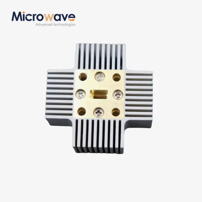
B2B procurement teams should prioritize manufacturers with CPW waveguide demonstrated expertise in RF and microwave PCB fabrication. Look for suppliers maintaining ISO 9001:2008 certification and RoHS compliance, as these standards indicate established quality management systems and environmental responsibility. Facilities equipped with advanced metrology tools, including automated optical inspection (AOI) systems and time-domain reflectometry (TDR) equipment, can verify dimensional tolerances and impedance accuracy critical to CPW performance. Manufacturing capability verification should extend beyond basic PCB fabrication to include assembly and testing services. Suppliers offering complete turnkey solutions from substrate selection through final electrical characterization streamline the procurement process and reduce coordination overhead between multiple vendors. Advanced Microwave Technologies Co., Ltd operates laboratories equipped with measurement equipment extending to 110 GHz, enabling comprehensive validation of fabricated CPW assemblies across millimeter-wave frequency ranges.
Cost Drivers and Procurement Strategies
Material selection represents a primary cost driver in curved CPW fabrication. Standard FR-4 substrates prove adequate for applications below 2 GHz but suffer from excessive loss tangent at higher frequencies. Specialized microwave laminates like Rogers RO4003C or Taconic TLY-5 deliver superior high-frequency performance at increased material costs. Engaging suppliers early in the design phase enables material selection optimization, balancing electrical performance against budget constraints. Manufacturing complexity scales with dimensional tolerances and feature density. Maintaining gap widths below 0.1mm demands tighter process control and more sophisticated fabrication equipment, directly impacting per-unit costs. Volume commitments provide leverage for negotiating favorable pricing, particularly when establishing long-term supply agreements. Buyers procuring components for satellite ground station deployments or defense programs should structure contracts incentivizing consistent quality and delivery performance over extended production runs.
Establishing Strategic Vendor Partnerships
Long-term relationships with specialized manufacturers yield substantial benefits beyond unit cost reduction. Collaborative partnerships enable concurrent engineering where supplier fabrication expertise informs design decisions early in development cycles, reducing iteration time and accelerating product introduction schedules. Technical support from manufacturing partners helps procurement teams navigate trade-offs between performance specifications, manufacturability, and cost targets. Quality assurance protocols should be formalized through detailed supplier agreements specifying inspection criteria, acceptance testing procedures, and traceability requirements. Defense and aerospace applications particularly demand rigorous documentation and supply chain transparency, aligning with AS9100D standards. Suppliers capable of supporting these requirements while maintaining competitive pricing and reliable delivery performance represent valuable strategic assets for organizations developing advanced microwave systems.
Best Practices and Tips for Optimizing Curved CPW Design in KiCad
Achieving reliable performance of a CPW waveguide from curved coplanar waveguide implementations requires attention to numerous design details that extend beyond basic geometric layout. These best practices reflect lessons learned across thousands of microwave circuit designs and help engineers avoid common pitfalls that compromise signal integrity.
Maintaining Dimensional Consistency
Variations in gap width or center conductor dimensions directly impact characteristic impedance, creating reflection points that degrade return loss and increase insertion loss. When drawing curved sections in KiCad, verify that track widths remain constant throughout the bend by measuring dimensions at multiple points along the arc. Small variations introduced during manual arc creation can accumulate to produce measurable impedance discontinuities. Consider implementing design rule checks (DRC) customized for your specific CPW geometry. Configure these rules to flag violations of minimum bend radius, gap spacing tolerances, and ground plane clearances. Catching these issues during layout prevents costly redesign iterations after fabrication. The investment in establishing comprehensive DRC rules pays dividends across multiple projects as design teams internalize best practices.
Ground Plane Optimization
While CPW structures theoretically operate without a backside ground plane, conductor-backed CPW (CBCPW) configurations offer advantages including improved mechanical strength, enhanced heat dissipation, and reduced susceptibility to electromagnetic interference from external sources. When implementing CBCPB designs, connect the top-side ground planes to the backside ground using via stitching at regular intervals not exceeding one-quarter wavelength at the highest operating frequency. Via placement near curved sections requires particular attention. Position vias to maintain ground potential equalization without creating parallel-plate waveguide mode resonances that can couple unwanted energy away from the intended CPW mode. Specialized RF simulation tools help optimize via placement patterns, though general guidance suggests spacing vias approximately every 0.1 wavelengths around curved sections.
Iterative Prototyping and Validation
Even carefully executed designs benefit from prototype fabrication and measurement validation before committing to volume production. Budget development timelines to accommodate at least one prototype iteration where measured electrical performance informs final design refinement. Time-domain reflectometry measurements identify impedance discontinuities and locate physical positions along the transmission line where improvements are needed. Vector network analyzer (VNA) S-parameter measurements provide a comprehensive characterization of insertion loss, return loss, and phase response across the operating frequency range. Compare measured results against simulation predictions to validate design methodologies and refine EM models for improved accuracy in subsequent projects. This iterative approach builds organizational expertise and reduces risk in critical applications where first-pass success carries high value. Incorporating these practices into your CPW design workflow establishes a foundation for consistent results and minimizes the technical risk inherent in high-frequency circuit development. Teams developing components for mission-critical satellite communication systems and defense radar applications particularly benefit from disciplined adherence to these methodologies.
Conclusion
Curved coplanar waveguide design in KiCad represents a practical approach to creating high-performance microwave circuits within compact form factors. The uniplanar architecture of CPW technology eliminates parasitic inductances associated with via grounding while enabling complex routing geometries essential for modern RF systems. Success requires careful attention to dimensional consistency, appropriate substrate selection, and validation through electromagnetic simulation and prototype measurement. Understanding comparative trade-offs between CPW and alternative transmission line technologies empowers procurement decisions aligned with application requirements and manufacturing capabilities. These design methodologies support the development of advanced microwave systems across satellite communications, aerospace, and defense sectors.
FAQ
1. How does KiCad handle impedance calculation for curved CPW sections?
KiCad provides PCB layout capabilities but lacks native electromagnetic simulation for impedance calculation. Designers must export Gerber files or other interchange formats to specialized EM simulation software like Sonnet or HFSS. These tools perform full-wave analysis accounting for curved geometry effects on characteristic impedance and enable S-parameter extraction for circuit-level simulation. The workflow involves iterating between KiCad layout refinement and EM simulation until performance targets are achieved.
2. What frequency range suits curved CPW implementations?
Coplanar waveguide technology operates effectively from DC through millimeter-wave frequencies exceeding 100 GHz. Practical upper frequency limits depend on fabrication tolerances, substrate losses, and dimensional precision. Standard PCB manufacturing maintains acceptable performance through approximately 40 GHz, while specialized processes using thin-film deposition on ceramic substrates extend capability beyond 100 GHz. The quasi-TEM propagation mode and low dispersion characteristics make CPW particularly attractive for wideband applications spanning multiple octaves.
3. Are curved CPW designs more expensive than standard microstrip?
Fabrication costs for curved CPW and microstrip designs prove comparable when using standard PCB processes, as both require similar substrate materials and metallization steps. CPW designs may reduce overall system costs by eliminating via drilling needed for microstrip ground connections, particularly in high-density layouts requiring numerous shunt components. The cost equation shifts toward CPW advantages when accounting for assembly complexity and the performance benefits of reduced parasitic inductance in millimeter-wave applications.
4. What design tools integrate best with KiCad for CPW development?
Engineers commonly pair KiCad with electromagnetic simulation platforms, including Sonnet Lite (free for moderate complexity designs), Keysight ADS with Momentum, and ANSYS HFSS. Python scripting bridges KiCad and simulation tools, enabling automated design exploration and optimization workflows. Open-source tools like OpenEMS provide accessible alternatives for teams requiring electromagnetic analysis without commercial software licensing. The key consideration is selecting simulation tools that accurately model planar transmission line structures across your target frequency range.
Partner with Advanced Microwave Technologies for Your CPW Component Needs
Advanced Microwave Technologies Co., Ltd brings over twenty years of specialized expertise in designing and manufacturing high-precision CPW waveguide components for demanding microwave applications. Our ISO 9001:2008 certified facilities house advanced measurement equipment extending to 110 GHz, enabling comprehensive validation of curved CPW assemblies for satellite communications, defense radar, and aerospace navigation systems. We offer complete OEM services encompassing design consultation, rapid prototyping, and volume production with strict quality control, ensuring dimensional tolerances within ±5%. Whether you require customized feed networks or complex antenna assemblies, our engineering team collaborates closely with your procurement and technical staff to optimize designs for performance and manufacturability. Global B2B clients benefit from our efficient supply chain, competitive pricing for volume commitments, CPW waveguide, and responsive technical support throughout product lifecycles. Connect with our team at craig@admicrowave.com to discuss how we can support your next microwave project with reliable CPW waveguide supplier capabilities and proven manufacturing excellence. Our 24-meter microwave darkroom facility enables precise far-field antenna measurements, ensuring your curved CPW components meet stringent specifications before deployment.
References
1. Simons, Rainee N. "Coplanar Waveguide Circuits, Components, and Systems." Wiley-IEEE Press, 2001.
2. Gupta, K.C., Ramesh Garg, Inder Bahl, and Prakash Bhartia. "Microstrip Lines and Slotlines, Third Edition." Artech House Publishers, 2013.
3. Wadell, Brian C. "Transmission Line Design Handbook." Artech House Microwave Library, 1991.
4. Collin, Robert E. "Foundations for Microwave Engineering, Second Edition." IEEE Press Series on Electromagnetic Wave Theory, 2001.
5. Jackson, David R. and Arthur A. Oliner. "Leaky-Wave Antennas." In Antenna Engineering Handbook, Fourth Edition, edited by John L. Volakis, McGraw-Hill Education, 2007.
6. Pozar, David M. "Microwave Engineering, Fourth Edition." John Wiley & Sons, 2011.