


The Ultimate Guide: Understanding Waveguide E Bend Dimensions, Types, and Performance
Picture this: You're integrating a critical satellite communication system or aerospace radar installation, and suddenly your waveguide routing hits a wall—literally. The flanges won't align, signal integrity is compromised, and the entire project timeline is at risk. This scenario haunts countless RF engineers who underestimate the complexity of waveguide E bend selection. The Ultimate Guide: Understanding Waveguide E Bend Dimensions, Types, and Performance delivers comprehensive insights into choosing, specifying, and implementing Waveguide E Bend solutions that guarantee reliable signal transmission while meeting the demanding requirements of modern microwave systems across satellite communications, defense, aerospace, and telecommunications infrastructure.
What is a Waveguide E Bend and Why Does It Matter?
The Waveguide E Bend represents a critical microwave component specifically engineered to redirect electromagnetic wave propagation within the E-plane, which corresponds to the electric field plane of the signal. Unlike simple metal tubes bent at arbitrary angles, a properly designed Waveguide E Bend maintains signal integrity while changing direction by carefully managing how the electric field distorts during the directional transition. This component earns its designation as an "E-bend" because it affects the electric field distribution as waves navigate through the bend, as opposed to H-bends which primarily influence the magnetic field component. In practical microwave systems, the Waveguide E Bend serves as the backbone of complex routing solutions where rigid waveguide installations must navigate around obstacles, connect misaligned equipment, or accommodate space constraints in densely packed electronic systems. The fundamental principle behind waveguide E bend operation involves bending the waveguide along its wider dimension, which is considered the "easy" direction from an electromagnetic propagation perspective. When electromagnetic waves encounter the bend, the electric field lines curve to follow the new path, and if the bend geometry is properly optimized, this transition occurs with minimal reflection, insertion loss, or mode conversion that could degrade system performance. The significance of Waveguide E Bend technology extends far beyond simple directional changes. These components directly impact critical performance parameters including voltage standing wave ratio (VSWR), insertion loss, phase tracking, and power handling capability. In satellite ground stations handling signals up to 110 GHz, even a poorly designed bend introducing 0.2 dB additional loss can significantly degrade link budgets and system margins. For phased array radar systems requiring precise phase relationships between array elements, waveguide E bend phase tracking accuracy becomes paramount, with deviations as small as two degrees potentially causing beam steering errors. Military surveillance systems operating in harsh environmental conditions demand waveguide E bends that maintain electrical performance across temperature extremes from negative fifty-five degrees Celsius to positive eighty-five degrees Celsius while resisting vibration, shock, and corrosion over decades of service life.

Waveguide E Bend Dimensions and Standard Specifications
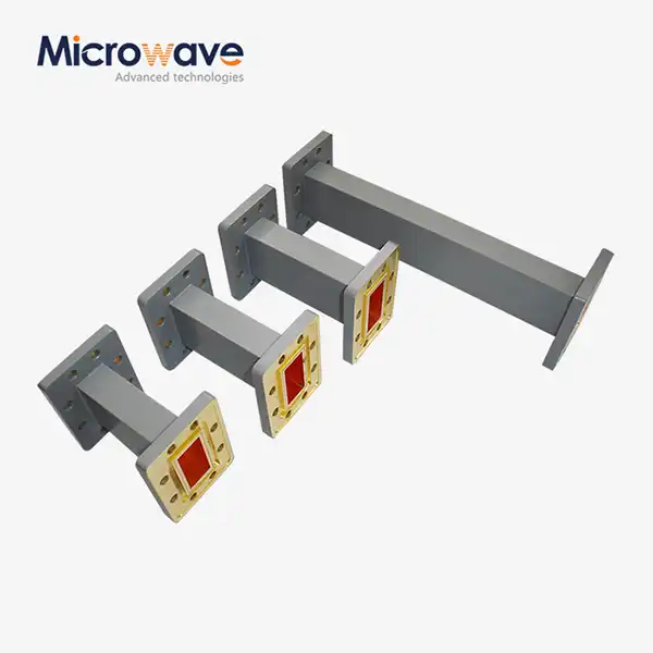
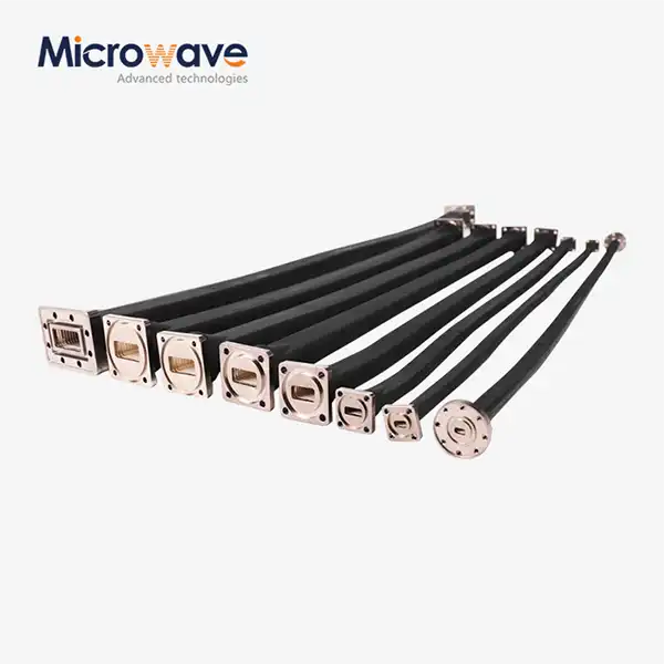
Understanding Waveguide E Bend dimensions begins with recognizing that these components follow standardized waveguide sizing conventions designated by WR (Waveguide Rectangular) numbers that indicate the waveguide's internal width in hundredths of an inch. The standard product line for waveguide E bends typically spans from WR10 through WR430, covering frequency ranges from approximately 1.7 GHz up to 110 GHz across the microwave and millimeter-wave spectrum. Each standard waveguide size corresponds to specific internal cross-sectional dimensions, with the width-to-height ratio carefully optimized, usually maintaining a two-to-one proportion that enhances single-mode propagation characteristics within the intended operating frequency band. For Waveguide E Bend components, the critical dimensional parameters extend beyond simple cross-sectional measurements to include bend radius, bend angle, and overall swept length. The bend radius represents the distance from the center of curvature to the centerline of the waveguide during the directional transition, and this parameter profoundly impacts electrical performance. General engineering practice dictates that waveguide E bend radius should exceed two wavelengths at the operating frequency to prevent significant reflections and maintain acceptable VSWR performance. For a WR90 waveguide operating at 10 GHz where the wavelength measures approximately 30 millimeters, the minimum bend radius should ideally exceed 60 millimeters to ensure optimal signal propagation characteristics. However, advanced design techniques incorporating sophisticated geometric optimizations enable tighter radius bends while maintaining excellent electrical performance through careful contouring of inner and outer corner geometries.
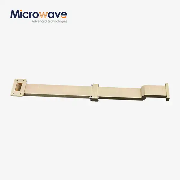
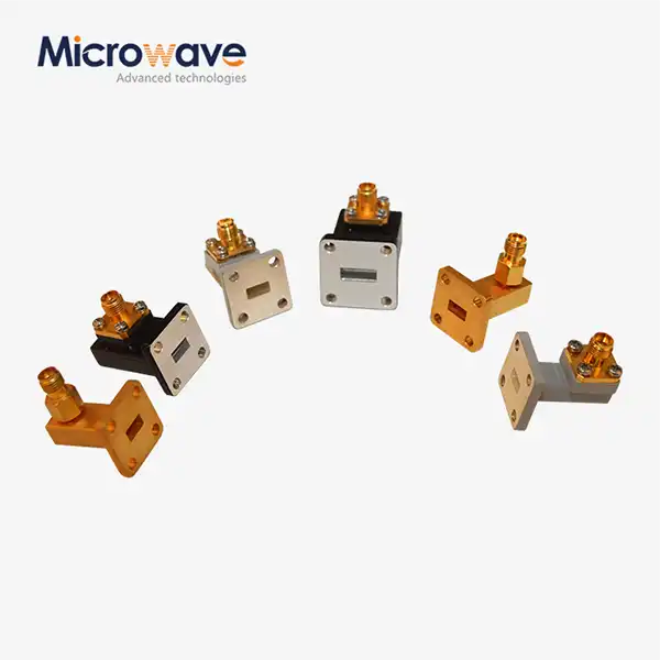
Standard Waveguide E Bend angles most commonly include 90-degree configurations for creating perpendicular routing paths, 45-degree bends for distributed direction changes, and custom angles tailored to specific installation requirements. The 90-degree Waveguide E Bend dominates practical applications due to its versatility in routing waveguide systems around corners and between equipment levels in rack-mounted installations. Advanced Microwave Technologies offers E-bends covering waveguide sizes WR10 through WR430 with multi-degree configurations, allowing system designers to specify precise angular transitions that optimize space utilization while maintaining signal integrity. Material specifications for Waveguide E Bend construction typically include high-conductivity aluminum alloys, brass, or copper, each selected based on application-specific requirements balancing weight, cost, machinability, and electrical conductivity. Surface finishing treatments dramatically impact performance, with silver or gold plating available to reduce surface resistance and minimize insertion loss, particularly at higher millimeter-wave frequencies where skin depth becomes vanishingly small. Flange specifications represent another critical dimensional consideration for Waveguide E Bend integration into larger waveguide systems. Standardized flange designs following military specifications ensure compatibility between components from different manufacturers and facilitate field assembly of complex waveguide networks. Precision-machined flanges maintain flatness tolerances typically within 0.001 inches to ensure consistent electrical contact and prevent leakage at flange interfaces. The bolt hole patterns, flange thickness, and gasket grooves all follow carefully controlled specifications that enable reliable mechanical and electrical connections capable of withstanding environmental stresses while maintaining electromagnetic performance over the component's operational lifetime.
Types of Waveguide E Bend Configurations
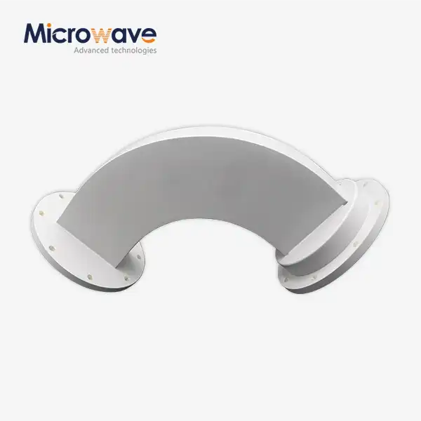
Waveguide E Bend configurations encompass several distinct design approaches, each optimized for specific application requirements, frequency ranges, and installation constraints. The radius bend represents the most fundamental type, featuring a smooth, constant-radius curve that gradually redirects the electromagnetic wave propagation direction. This configuration excels in applications demanding the absolute lowest insertion loss and best VSWR performance because the gradual curvature minimizes field distortion and reflection. Advanced Microwave Technologies manufactures radius E-bends with carefully controlled bend radii exceeding two wavelengths, employing precision manufacturing techniques that maintain dimensional tolerances ensuring consistent electrical characteristics. The manufacturing process for radius waveguide E bends involves specialized forming equipment that bends the waveguide structure while maintaining constant internal cross-sectional dimensions, preventing bumps, dents, or discontinuities that would appear as impedance mismatches causing signal reflections. Miter bend configurations offer an alternative approach for applications requiring sharper directional transitions within constrained spaces where gentle radius bends cannot physically fit. The miter Waveguide E Bend employs one or more angled reflecting surfaces, typically at 45-degree orientations, to redirect electromagnetic wave propagation through internal reflections rather than gradual curvature. Single miter designs feature a direct 90-degree transition using a single 45-degree reflecting surface, though this configuration can exhibit frequency-sensitive behavior and challenging impedance matching at the corner junction. Double miter E-bends incorporate two consecutive 45-degree bends separated by a straight waveguide section, and this configuration enables superior electrical performance by strategically spacing the reflecting surfaces an odd multiple of quarter wavelengths apart, causing reflections generated at the first corner to cancel reflections from the second corner through destructive interference. This cancellation mechanism results in lower VSWR across the operating bandwidth compared to single miter designs while still accomplishing sharp 90-degree turns within much smaller physical footprints than radius bends.
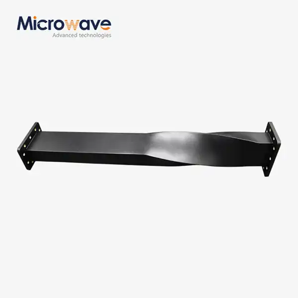
Compound waveguide E bends represent sophisticated configurations combining multiple angular transitions to achieve complex routing paths within a single integrated component. These specialized designs might incorporate combinations of different bend angles—perhaps a 45-degree bend followed by a 90-degree transition—enabling waveguide routing that navigates around multiple obstacles or connects equipment at non-standard orientations. Advanced Microwave Technologies provides custom compound E-bend designs tailored to specific installation challenges, leveraging extensive engineering expertise and advanced electromagnetic simulation tools to optimize geometry for minimal loss and excellent VSWR across the required frequency range. The design process for compound bends requires careful attention to the spacing and orientation of each transition to prevent unintended resonances or mode conversion effects that could degrade electrical performance. Offset Waveguide E Bend configurations serve specialized applications requiring both directional change and lateral displacement of the waveguide centerline. These components prove invaluable when connecting flanges that are offset in two dimensions, enabling alignment correction without requiring multiple separate bend components. The offset E-bend typically incorporates a combination of bends and straight sections arranged to produce the desired lateral displacement while maintaining the input and output flanges in parallel orientations. Manufacturing these complex geometries demands exceptional precision and sophisticated tooling to ensure all internal surfaces remain smooth and dimensionally accurate, preventing reflections and maintaining low insertion loss across the operating bandwidth.
Performance Parameters and Testing of Waveguide E Bend
Understanding Waveguide E Bend performance requires comprehensive knowledge of multiple interconnected electrical parameters that collectively determine component suitability for demanding microwave applications. Voltage Standing Wave Ratio (VSWR) stands as perhaps the most fundamental performance metric, quantifying the level of impedance matching between the waveguide E bend and the connected transmission line system. VSWR values approaching 1.0:1 indicate nearly perfect impedance matching with minimal reflections, while higher VSWR values signal increasing reflection levels that reduce power delivered to the load and can potentially damage sensitive source equipment. High-quality waveguide E bends from Advanced Microwave Technologies typically achieve VSWR specifications of 1.15:1 or better across the full waveguide operating bandwidth, with premium designs reaching performance levels below 1.10:1 through sophisticated geometric optimization and precision manufacturing techniques. Insertion loss represents another critical Waveguide E Bend performance parameter, quantifying the signal power reduction as electromagnetic waves propagate through the component. This loss arises from multiple mechanisms including resistive losses in the waveguide walls due to finite conductivity, dielectric losses if any insulating materials contact the electromagnetic fields, and radiation losses if the component geometry permits field leakage. Well-designed waveguide E bends typically exhibit insertion loss below 0.1 dB at mid-band frequencies, though losses increase toward band edges and at higher millimeter-wave frequencies where skin depth decreases and surface roughness effects become proportionally more significant. Surface finishing treatments using silver or gold plating substantially reduce insertion loss by minimizing surface resistance, particularly important for Waveguide E Bend components operating at frequencies approaching 110 GHz where even minor surface imperfections can cause measurable performance degradation.
Phase tracking accuracy assumes critical importance in Waveguide E Bend applications involving phased array antennas or interferometric measurement systems where precise phase relationships between multiple signal paths must be maintained. Manufacturing variations in bend geometry, material properties, or surface finish can introduce phase deviations between nominally identical waveguide E bend components, causing beam steering errors in phased arrays or measurement uncertainties in precision test systems. Advanced Microwave Technologies maintains phase tracking tolerances within plus or minus two degrees between matched pairs of E-bends through rigorous manufacturing process controls and comprehensive electrical testing using network analyzers capable of characterizing phase response up to 110 GHz frequencies. Power handling capability determines the maximum RF power level that a Waveguide E Bend can safely transmit without risk of thermal damage, voltage breakdown, or passive intermodulation generation. The power handling limit depends on multiple factors including material properties, surface finish quality, cooling provisions, and the operating frequency. Waveguide E Bend components fabricated from high-conductivity copper with precision surface finishes can handle kilowatt-level continuous wave power in lower frequency bands, though power handling capability decreases at higher frequencies due to increased current density in the smaller waveguide cross-sections. Applications such as high-power radar transmitters or industrial heating systems require careful attention to waveguide E bend power handling specifications to prevent component failure or performance degradation during operation.
Comprehensive testing of Waveguide E Bend components employs sophisticated measurement equipment and rigorous test procedures to verify electrical performance across all relevant parameters. Vector network analyzers calibrated up to 110 GHz enable precision characterization of VSWR, insertion loss, return loss, and phase response across the full operating bandwidth. Advanced Microwave Technologies' laboratories feature state-of-the-art measurement capabilities including the remarkable 24-meter microwave darkroom equipped with an Antenna Plane Near and Far Field Measuring Recombination Chamber, providing unrivaled facilities for comprehensive component testing and validation. Dimensional inspection using coordinate measuring machines verifies that manufactured parts meet exacting geometric tolerances, while visual examination assesses surface finish quality and detects any manufacturing defects. Environmental testing subjects waveguide E bend components to temperature cycling, vibration, humidity, and other stresses representing operational conditions, ensuring reliable performance throughout the component's service life.
Applications and Selection Criteria for Waveguide E Bend
Waveguide E Bend applications span a remarkable range of critical technologies where reliable microwave signal transmission proves essential for system operation. Satellite communication ground stations represent a major application domain, where waveguide E bends route high-frequency signals between antenna feeds and receiver/transmitter equipment often separated by substantial distances and requiring multiple directional changes to navigate building structures and equipment racks. These installations demand Waveguide E Bend components exhibiting exceptional electrical performance to preserve the weak signals received from distant satellites, with insertion loss specifications typically below 0.08 dB and VSWR better than 1.12:1 to maintain adequate link margins for reliable data transfer. The frequency range spanning C-band, X-band, Ku-band, and Ka-band satellite communications requires waveguide E bends covering standard sizes from WR229 down to WR28, each precision-engineered for optimal performance within the specific frequency allocation. Aerospace and defense radar systems employ Waveguide E Bend components extensively in both airborne and ground-based installations where space constraints, weight limitations, and extreme environmental conditions impose demanding requirements. Air traffic control radar systems utilize E-bends to route signals between the rotating antenna assembly and stationary processing equipment, requiring specialized rotary joint interfaces combined with waveguide bends that maintain signal integrity despite continuous rotation and vibration. Military surveillance radars operating across harsh temperature ranges from arctic cold to desert heat demand waveguide E bend designs incorporating materials and surface treatments that resist corrosion while maintaining consistent electrical performance across the full environmental envelope. Advanced phased array radar systems for missile defense or space surveillance applications require matched sets of Waveguide E Bend components exhibiting exceptional phase tracking accuracy, with deviations below one degree between elements to enable precise beam steering and target discrimination capabilities.

Telecommunications infrastructure networks increasingly employ Waveguide E Bend technology in millimeter-wave backhaul links and 5G base station installations where high-frequency operation enables greater bandwidth and reduced antenna size. The migration toward millimeter-wave frequencies above 24 GHz for next-generation wireless systems creates growing demand for waveguide components including E-bends optimized for WR42, WR28, and smaller sizes operating up to 110 GHz. These applications require Waveguide E Bend designs balancing electrical performance with cost-effectiveness and ease of installation, driving innovations in materials, manufacturing processes, and component integration that reduce system deployment time and expense while maintaining the reliability essential for commercial telecommunications infrastructure.
Selection of appropriate Waveguide E Bend components for specific applications requires systematic evaluation of multiple criteria encompassing electrical requirements, mechanical constraints, environmental conditions, and cost considerations. The frequency range represents the foundational selection parameter, determining the appropriate waveguide size from the WR10 through WR430 standard series available from Advanced Microwave Technologies. Engineers must ensure the selected waveguide size operates comfortably within its recommended frequency band, avoiding operation near cutoff frequency where propagation becomes unstable or at excessively high frequencies where higher-order modes might propagate, causing multimode interference. Electrical performance specifications including VSWR, insertion loss, and power handling must meet or exceed system requirements with appropriate margins, recognizing that component specifications typically represent nominal values with manufacturing tolerances that should be considered during system design. Mechanical integration factors including bend angle, bend radius, flange type, and overall component dimensions must be carefully evaluated against installation constraints and mounting provisions. Custom bend angles beyond the standard 45-degree and 90-degree configurations enable optimized routing that minimizes the number of components while achieving required spatial arrangements, potentially reducing system cost and complexity. Environmental specifications encompassing operating temperature range, humidity resistance, vibration tolerance, and corrosion protection must align with anticipated deployment conditions, particularly for outdoor installations or mobile platforms subjected to severe environmental stresses. Advanced Microwave Technologies provides comprehensive technical support assisting customers in selecting optimal Waveguide E Bend configurations for their specific applications, leveraging over two decades of manufacturing experience and deep engineering expertise in microwave component design.
Conclusion
Selecting high-performance Waveguide E Bend components demands careful attention to dimensions, types, and electrical specifications that collectively determine system success in demanding microwave applications.
Cooperate with Advanced Microwave Technologies Co., Ltd.
As a China Waveguide E Bend factory with ISO 9001:2015 certification and over twenty years of manufacturing excellence, Advanced Microwave Technologies Co., Ltd stands ready to support your most challenging microwave system requirements. Our China Waveguide E Bend supplier capabilities encompass standard product lines covering WR10 through WR430 sizes plus comprehensive OEM services delivering custom solutions tailored to your unique specifications. Whether you need China Waveguide E Bend manufacturer expertise for prototype development or China Waveguide E Bend wholesale volumes for production deployments, our vertically integrated facilities equipped with advanced measurement systems up to 110 GHz ensure consistent quality and rapid delivery. Explore our Waveguide E Bend for sale catalog featuring competitive Waveguide E Bend price structures without compromising the High Quality Waveguide E Bend performance your applications demand. Contact craig@admicrowave.com today to discuss your waveguide requirements with our experienced engineering team and discover how our perfect supply chain system, professional R&D capabilities, and strong after-sales support can accelerate your project success.
References
1. Military Standardization Handbook for the Fabrication of Rigid Waveguide Assemblies (MIL-HDBK-660B), U.S. Department of Defense
2. Pozar, David M. "Microwave Engineering Fourth Edition", John Wiley & Sons
3. Collin, Robert E. "Foundations for Microwave Engineering Second Edition", IEEE Press
4. Saad, Theodore S. "Microwave Engineers' Handbook Volumes 1 and 2", Artech House