





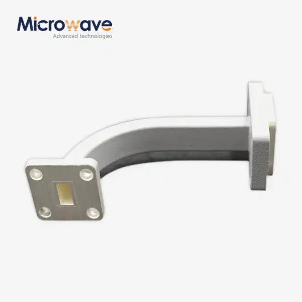
Waveguide E Bend
Waveguide E Bend Components for High-Power RF Signal Routing
Waveguide E Bend is a passive microwave component that redirects RF signal propagation by curving along the plane of the electric field. The wide wall bends in this shape, but the thin wall stays flat. This keeps the dominant TE10 mode pure with little insertion loss. Advanced Microwave Technologies (ADM) has a standard line of products that includes waveguides in sizes WR10 to WR430. For aircraft, defence, and satellite communication uses, you can ask for custom bend angles, non-standard sizes, and multi-combination assemblies.
What Is a Waveguide E Bend and How Does It Work?
In contrast to coaxial cables, a product moves strong radio frequency signals through mechanical parts that are limited in space, like radar nose cones or satellite payloads, without causing major impedance mismatches or high VSWR.
This is the most important design parameter: the swept radius. Instead of a sharp corner, a swept radius that goes beyond one wavelength keeps the phase stable and reduces reflections. This makes high-frequency transmission lines less likely to lose power. It is also possible to change the internal geometry to find a good balance between small size and good electrical performance, which is a common need in defence and aerospace hardware.
Materials and Construction
ADM's product components are manufactured from precision-grade materials selected for their electrical and mechanical properties:
· Oxygen-Free High Conductivity (OFHC) Copper — lowest resistive loss, suited for high-frequency bands
· Aluminum 6061 — lightweight option for airborne or space-based platforms
· Brass — cost-effective for ground-based or laboratory applications
Internal surfaces are finished to a roughness of Ra < 1.6 µm to reduce skin-depth losses. Silver or gold plating is applied internally to improve conductivity, which is particularly relevant at Ka-band and W-band frequencies where the skin effect concentrates RF current at the metal surface.
External surfaces are passivated with chromate conversion coating for corrosion resistance, suitable for marine radar, outdoor systems, and harsh-environment deployments.


Key Technical Specifications
Parameter | Specification |
Waveguide Size Range | WR10 to WR430 |
VSWR | < 1.10:1 (Return Loss > 26 dB) |
Insertion Loss | < 0.05 dB (typical) |
Internal Surface Roughness | Ra < 1.6 µm |
Frequency Coverage | X, Ku, Ka, W bands (EIA/MIL standards) |
Power Handling | kW (CW) to MW (Peak), depending on waveguide size |
Flange Standard | UG-39/U and other standard configurations |
Material Options | OFHC Copper, Aluminum 6061, Brass |
Plating Options | Silver, Gold |
External Finish | Chromate conversion coating |
Custom Configurations | Multi-degree bends, non-standard sizes, combination assemblies |
Application Scenarios
When low-loss RF routing in small spaces is a strict design requirement, waveguide E bend components are used.
Airborne Fire Control Radar: There isn't a lot of room in the nose cone of a fighter plane. When a transmitter sends a high-power pulse, E-bends direct it to the planar array antenna. To keep phase alignment, parts must stay the same size even when subjected to high G-forces and vibration.
High-Throughput Satellite (HTS) Payloads: E-bends are built into High Power Amplifier networks at the Ka-band and Ku-band frequencies. These parts have to work with a lot of heat and meet the electrical and mechanical needs of the satellite payload environment.
Medical Linear Accelerators (LINAC): E-bends channel RF power from Klystron sources to the structure that speeds up particles. To keep arcing from happening during high-energy pulse transmission used in cancer treatment systems, the environment needs to be compatible with ultrahigh vacuum.
Quality Control and Inspection Process
Every time ADM ships a product, it goes through a structured inspection process that checks for both electrical and mechanical issues.
Vector Network Analyser (VNA) Sweep: A full-band VSWR and insertion loss sweep is done on every unit. Response anomalies show problems on the inside of the surface or the wrong bend geometry.
CMM Dimensional Verification: Coordinate measuring tools are used to check the flatness of the flange and the size of the opening. RF leakage and arcing happen at flange joints where the flanges don't match.
Borescope Internal Inspection: The internal bend radius is visually inspected for burrs, pits, or plating irregularities that can act as hotspots for RF breakdown under high power.
Pressure and Leak Testing: For systems that use dry nitrogen or SF6, each unit goes through pneumatic or hydrostatic leak tests to make sure that the braze joints are hermetically sealed.
Salt Spray Testing (ASTM B117): Marine radar, shipboard, and outdoor equipment can use external plating that has been tested against salt fog.
Why Choose ADM for Waveguide Components?
Antenna Plane Near and Far Field Measuring Recombination Chamber and a 24-meter microwave darkroom are run by ADM. The test frequency range goes from 0.5 GHz to 110 GHz. This building inside the company lets us test Waveguide E Bend assemblies and antenna systems correctly in a controlled environment.
In Xi'an, there are engineering teams and a specialised R&D lab. There are also branch offices in Chengdu, Beijing, Tianjin, and Shijiazhuang. Customers in the aerospace, defence, satellite communication, and test and measurement industries buy microwave parts from ADM. They can choose from standard catalogue items or fully customised parts.
If you need a certain frequency band, power level, or flange, you should talk to the engineering team about your configuration options.
FAQ
Q: What's the difference between a H Bend and an E Bend in a waveguide?
A: The electric field vector is turned by an E-bend that curves along the wide wall (E-plane). Along the thin wall, there is an H-bend (H-plane). An E-bend seems to flatten out, while an H-bend seems to turn on its side.
Q: What's the point of the bend radius?
A: The radius determines how well the impedance matches. Reflections are kept to a minimum by sweeping the radius beyond one wavelength. If the radius is too small and there is no mitre correction, VSWR goes up, sending power back to the source.
Q: If I have a product, can it pass DC signals?
A: No, waveguides are not like that. They work as high-pass filters and need to be the right size in terms of half-wavelengths in order to send RF energy. They can't send DC or any other signal below the frequency they block.
Q: What effect does interior plating have on performance?
A: Silver or gold treatment on the inside walls of the conductor lowers resistive heating and insertion loss because RF current moves on the surface of the conductor. When the skin is very thin, like at the Ka-band and W-band, this effect is stronger.
Q: What makes arcing happen inside a waveguide bend?
A: High voltage gradients at sharp internal edges, debris, or moisture can cause arcing. It can't happen because the insides are smooth, the assembly conditions are controlled, and the waveguide is pressed with dry air or nitrogen when needed.
Q: What kinds of custom settings does ADM allow?
A: ADM can handle bends of more than one degree, waveguide sizes that aren't in the WR10–WR430 range, and combination assemblies. Give the engineering team your frequency band, power level, and flange type so they can talk about your choices.
Contact Us
Send your technical requirements for Waveguide E Bend to craig@admicrowave.com. Include your frequency band, power level, and flange standard for a faster response.