


Coplanar Waveguide Design for Your RF PCB
Coplanar waveguide transmission line designs are an important part of current RF printed circuit board design, especially for high-frequency uses like radar systems, satellite communications, and advanced telecom infrastructure. A coplanar waveguide is different from traditional microstrip designs because it puts the signal line and ground planes on the same PCB surface. This gives you more control over how the electromagnetic field is distributed and reduces the amount of energy that is lost. This way of designing has measured benefits in terms of impedance consistency, heat management, and how easy it is to integrate with surface-mount components. These benefits are very important when your application needs to reliably send signals from the X-band to the Ka-band.
Understanding Coplanar Waveguide Fundamentals
The science behind how coplanar waveguide structures work is based on quasi-TEM mode propagation, in which electromagnetic fields are mostly present between the middle conductor and the ground planes next to it. In contrast to microstrip setups, this design keeps fields closer to the substrate surface, which lowers dielectric losses and makes phase velocity more stable over a wide frequency range.
Structural Anatomy and Impedance Control
In CPW designs, characteristic impedance is affected by three physical factors: the center conductor width (W), the gap between the conductor and ground planes (S), and the substrate dielectric constant (εr). The connection is based on complicated conformal mapping formulae, but in practice, the goal is usually 50 ohms of impedance to match standard RF system interfaces. Precision in keeping W/S ratios during manufacturing has a direct effect on VSWR performance, which is a requirement that defense companies look over very carefully when choosing suppliers.
Electromagnetic Mode Behavior
Dominant mode purity is still important for knowing how a circuit will work. Higher-order modes are naturally stifled in CPW designs because the ground plane is close by. However, at changes and bends, you need to pay close attention to discontinuities. For most substrate materials, dispersion properties stay pretty flat below 40 GHz. This means that CPW can be used in wideband applications where group delay uniformity is important. Our test rooms have vector network monitors that are set to 110 GHz, and these values are always checked during prototype validation.
Loss Mechanisms and Mitigation Strategies
CPW performance is affected by three main types of loss: conductor loss due to metal resistance, dielectric loss tangent in base materials, and radiation loss at breaks. For millimeter-wave designs, electropolished or rolled copper foils are needed because conductor losses above 20 GHz are mostly caused by the Coplanar waveguide roughness of the copper surface. When choosing a substrate, you have to weigh the security of the dielectric constant against the loss tangent. For example, PTFE materials have a loss tangent below 0.002, while ceramics like alumina are better at conducting heat for handling high power. To stop radiation, you need to be careful with the layout, like making sure there aren't any sudden changes in resistance and that the ground plane stays connected. Both the design optimization and supplier approval methods are based on these scientific principles. When buying teams, look at different makers; they should make sure that they can control trace geometries to within ±10 microns and that they can get low-loss substrate materials that have been tested for their electrical qualities across your working frequency range.
Best Practices and Design Principles for CPW on RF PCBs
To turn theoretical coplanar waveguide benefits into hardware that can be built, strict obedience to layout rules and testing methods is needed. Design discipline stops costly re-designs and speeds up qualification times, which are measures that matter when the competition is putting pressure on your product plan.
Critical Dimensional Parameters
The main factors that affect resistance are conductor width and gap spacing. When spaces are smaller, capacitance goes up, and impedance goes down. When wires are smaller, inductance goes up. There are practical limits to what can be made. Most PCB makers can safely make 4-mil traces and spaces, but millimeter-wave designs may need 2-mil features, which means using different methods and tighter production tolerances. Field confinement and diffusion are affected by the thickness of the substrate. Thinner surfaces lower loss, but make it harder to handle during assembly. Thick materials make mechanical processing easier but raise the risk of mode conversion at higher frequencies. Thicknesses of 10 to 20 mils are standard for most uses up to the X-band. Thinner materials are only used for the Ka-band and beyond.
Electromagnetic Simulation for Design Validation
Modern EM modeling tools let you get a good idea of how something will work before you actually make it. Ansys HFSS and Keysight ADS are two platforms that use finite element or method-of-moments methods to solve Maxwell's equations across your structure and get S-parameters, impedance profiles, and field distributions. To set up a simulation correctly, you need to get exact values for the dielectric constant, loss vector, and copper conductivity from the supplier's datasheets or by measuring the material directly. Simulations help find efficiency problems early in the planning process. When there are breaks at T-junctions and turns, impedance mismatches happen, which cause return loss peaks. VSWR stays below 1.3:1 across all working bandwidths when these transitions are optimized with chamfering or correction stubs. Comparing the model to measurement data from our 24-meter anechoic chamber shows that it is accurate and increases trust in design changes that are based on simulations.
Manufacturing Considerations and Quality Assurance
Design for manufacturing principles help keep production problems that hurt electrical performance to a minimum. Keeping the copper weights the same across the screen makes sure that the circuit losses are the same. Choosing plated-through-hole vias with the right aspect ratios keeps reliability from breaking down during thermal cycling. This is especially important for aircraft uses that experience wide temperature changes. Optical checking and electrical tests should be used in quality control to make sure that the dimensions are correct. Time-domain reflectometry finds breaks in impedance along transmission lines, and readings from a network analyzer show that the insertion loss and return loss meet the requirements. Working with makers who are certified to ISO 9001:2015 and can show that they use statistical process control is a good way to make sure that the quality of each production lot stays the same. Our engineering team had to come up with a tricky coplanar waveguide design for a Ka-band satellite ground terminal that had to have an insertion loss below 0.5 dB/inch across 27–31 GHz. Rogers RO3003 was chosen as the substrate because it has stable dielectric qualities and a low loss slope. Simulations expected performance margins, but the first samples recorded 0.7 dB/inch because the copper surface was rougher than the models thought it would be. When roughness dropped from 5 microns to 2 microns RMS when reverse-treated foil Coplanar waveguide was used, the observed loss reached 0.45 dB/inch, which met program standards.
Procurement Guide: Sourcing High-Quality Coplanar Waveguide Components
To strategically source RF PCBs and related parts, you need to know what the suppliers can do, how to track materials, and the total cost of ownership, which goes beyond unit price. To make supply lines more secure, partners must be evaluated on a number of factors that affect the success of the program.
Manufacturer and Supplier Qualification Criteria
Checking a supplier's professional skills is the first step in evaluating them. Can the maker keep 3-mil line lengths and spaces the same every time? Do they offer services with limited resistance and clear tolerance limits? Asking for process capability studies (Cpk data) for important aspects shows you the statistical control levels and tells you what kind of return you can expect from your designs. Material tracking makes sure that custom laminates are real. Sometimes, fake substrates get into supply chains and replace better materials that break while they're being used. Suppliers you can trust give you certificates of conformance that connect the lot numbers of materials to test reports from the manufacturer that show their insulating properties. RoHS compliance paperwork confirms that the processing does not contain lead, which is necessary for commercial aircraft and entering the EU market.
Custom Fabrication Versus Catalog Components
Off-the-shelf waveguide systems work well for common uses where quick placement is more important than being able to change the size of the components. Catalog parts from well-known makers can be shipped within days, which speeds up the building of prototypes and lowers the costs of buying things. But performance is harmed when common settings don't exactly match the way your system is built. Custom construction gives you the best performance that fits your exact needs. By changing the shapes of the powers, choosing the right substrates, and building changes into the assembly itself, you can get rid of the need for external connections that cause losses and reflections. In exchange, lead times are longer—usually 4 to 6 weeks for PCB fabrication plus extra time for testing and assembly—and unit costs are higher because NRE charges for setup and tooling. The cost of mass production changes the economy in favor of custom methods. When NRE is spread out over thousands of units, piece prices drop below stock options while electrical performance improves. For budget security, procurement strategies should make accurate predictions of yearly demand and negotiate framework deals that lock in prices and capacity.
Critical Purchasing Considerations
How well a connector works directly impacts how accurate measurements are and how reliable they are over time. Millimeter-wave frequencies don't affect the phase stability or low VSWR of precision SMA, 2.92mm, and 2.4mm connections, but there are a lot of fakes on the market with worse standards. Getting connectors from approved distributors like Digi-Key or Mouser, or straight from makers like Southwest Microwave, lowers the chance that low-quality parts will mess up your assembly. The best use of buying funds is to understand how prices change over time. PCB costs go up or down depending on how efficiently panels are used. Designs that make the most of the boards on a panel lower unit costs. Substrate material makes up 30–40% of the total cost of a PCB, so choosing the right material can have a big effect on the cost. Combining orders from different programs gives sellers more power when negotiating with suppliers, but they have to weigh the costs of keeping goods against price cuts. Another type of equipment that needs to be bought that affects coplanar waveguide development processes is test equipment. Vector network analyzers tuned over your working frequency range check the S-parameters, and time-domain reflectometry finds problems with the impedance. Keysight, Rohde & Schwarz, and Anritsu are the biggest names in this field. Their tools are known to be accurate and can be calibrated to national standards. For labs with limited funds, the used equipment market offers cheaper options, but testing currency is still necessary for accurate measurements. Advanced Microwave Technologies Co., Ltd. works with experienced PCB makers who focus on making precise parts and RF substrates. Material approvals and process checks are part of our supply chain. They make sure that parts meet the quality standards for aerospace and defense. This infrastructure can handle both small prototypes for testing new ideas and large production runs for putting systems into use. It also has expert support that can help with design and production issues at all stages of a program's lifecycle.
Advanced Topics and Future Trends in Coplanar Waveguide Technology
Coplanar waveguide powers are changing, and more uses are becoming possible thanks to new developments in materials science, fabrication processes, and modeling methods. By keeping up with new developments, buying and engineering teams can take advantage of better performance and lower costs as technologies grow.
Materials Innovation and Performance Enhancement
Liquid crystal polymer substrates are a new Coplanar waveguide and an interesting discovery. They have very low loss tangents (below 0.002) and can be processed organically. Flexible coplanar waveguide circuits that can bend around curved surfaces are made possible by LCP materials. This makes them useful for conformal antenna arrays on the fuselages of airplanes or missiles. Above 200°C, thermal stability is still an issue, which limits its use in high-power transmit chains. However, receive-path applications quickly benefit from lower noise levels. Additive manufacturing methods could be useful for making quick prototypes and small amounts of products. Aerosol jet printing puts 50-micron-thick conductive lines directly on materials, skipping the photolithography steps and cutting the time it takes to make changes from weeks to days. Conductor resistivity is currently 2-3 times higher than that of bulk copper, but researchers working on nanoparticle inks hope to reach performance balance within a few years.
Expanding Application Domains
As 5G networks get denser, there is a greater need for small, high-performance RF front-ends that combine coplanar waveguide structures with active devices. Millimeter-wave frequencies between 28 GHz and 39 GHz need transmission lines with tight impedance control and low loss. CPW is great at meeting these needs. CPW feed networks are used by phased array antennas for beamforming to send data to hundreds of elements while keeping the phase synchronization. In microwave photonics, CPW electrodes are used to change laser diodes at microwave speeds, combining the optical and RF domains. These systems can reach bandwidths of more than 100 GHz, which lets them handle very fast data and the creation of radar waveforms. CPW is the best transmission line for these mixed designs because it has low dispersion and can be integrated with optical waveguides.
Simulation and Measurement Advancements
Machine learning algorithms now help electromagnetic simulation by making predictions about design outcomes from small amounts of training data and using automatic search methods to find the best geometries. These tools save engineers time because they explore design spaces faster than doing iterations by hand. This is especially helpful when there are a lot of speed limits to meet at once. Instruments for measuring are moving toward terahertz frequencies, and network monitors and probe stations can make bandwidths wider than 500 GHz helpful. Characterizing coplanar waveguide behavior at these extremes reveals loss mechanisms masked at lower frequencies, informing material selection and layout practices for next-generation systems operating in the sub-millimeter-wave spectrum. Through our study partnerships with universities and defense labs, we stay on top of the newest ideas before they're ready for sale. We can help our clients choose future-proof systems that can adapt to changing technologies without having to be redesigned. This protects their R&D investments and helps them stay ahead of the competition.
Conclusion
Coplanar waveguide designs have real benefits in RF PCB uses where signal integrity, thermal performance, and the ability to make the same system over and over again are important for system success. By understanding the electromagnetic principles that control CPW behavior, weighing the pros and cons of different transmission lines, and using focused design practices, engineering teams can get the most out of this tried-and-true architecture. Strategic buying methods combine technical needs with the skills of suppliers, the ability to track materials, and the total cost of the purchase. Complex RF supply chains come with risks that can be reduced by working with makers that show process control, quality certifications, and quick expert support. Staying up to date on new materials and manufacturing methods is important to make sure that your designs stay competitive and that your buying strategies adapt to how the market is changing.
FAQ
What advantages do coplanar waveguides offer compared to microstrip lines?
Signal and ground wires are placed on the same PCB surface by coplanar waveguide structures. This makes it easier to integrate components and lowers the parasitic inductance that comes from via transitions. This design makes it easier to test probes during development and better separates transmission lines that are next to each other. CPW structures have less dispersion over a wide range of frequencies than microstrip structures, especially above 20 GHz, where keeping phase uniformity is very important. Better thermal control is achieved because heat moves straight through the substrate, not through vias to buried ground planes.
How do electromagnetic simulation tools improve CPW design accuracy?
Advanced computer tools can solve Maxwell's equations across the shape of your PCB and predict S-parameters, impedance profiles, and field patterns before the board is even made. For accurate models, you need to know the exact dielectric constant, loss slope, and copper conductivity of the material. You can get these from source datasheets or by measuring the material. Simulation finds performance problems like impedance discontinuities at bends and joints. This lets you improve performance by changing the shape before you spend time and money on prototypes. When simulated and measured results are linked, it increases trust in design predictions, which cuts down on iteration cycles and speeds up approval times.
What criteria should buyers evaluate when selecting CPW PCB manufacturers?
Before you judge a provider, you should check their ability to control dimensions. You can do this by asking for process capability studies that look at line width and spacing limits. Material traceability makes sure that custom laminates are real by connecting lot numbers to test data from the maker on certificates of conformance. Quality standards, such as ISO 9001:2015, show that processes are controlled in a planned way and that they are always getting better. How quickly technical help responds is important when answering questions about design or fixing problems with manufacturing. A history of delivery performance and clear capacity sharing helps buyers handle scheduling risks across multiple projects.
Partner with ADM for Superior Coplanar Waveguide Solutions
Advanced Microwave Technologies Co., Ltd has been making RF components for more than 20 years and can help clients who need reliable coplanar waveguide designs and high-quality Coplanar waveguide production. Our ISO 9001:2015-certified facilities have advanced measuring tools up to 110 GHz and strict quality control to make sure that your specs are translated into consistent production hardware. Our engineering team is here to help you from the first idea to the finished product, whether you need custom waveguide systems, test PCBs to make sure the design works, or mass production with clear material tracing.
We work with defense providers, companies that put together satellite systems, companies that build telecom infrastructure, and research schools that need mission-critical RF. Our global shipping network makes sure that deliveries happen on time, and low prices and good supply chain management give you real value. We are a reliable coplanar waveguide seller with a track record of strong technical knowledge and top-notch manufacturing. We help our clients make difficult purchasing choices and reach their engineering goals.
Get in touch with craig@admicrowave.com right away to talk about your project needs and find out how our services can help you cut down on development time while still meeting the quality standards your apps need.
References
1. Simons, Rainee N. Coplanar Waveguide Circuits, Components, and Systems. Wiley-IEEE Press, 2001.
2. Wadell, Brian C. Transmission Line Design Handbook. Artech House Publishers, 1991.
3. Gupta, K. C., Ramesh Garg, Inder Bahl, and Prakash Bhartia. Microstrip Lines and Slotlines. Artech House Publishers, 1996.
4. Pozar, David M. Microwave Engineering, 4th Edition. Wiley, 2011.
5. Edwards, Terry C., and Michael B. Steer. Foundations for Microstrip Circuit Design. Wiley, 2016.
6. Bahl, Inder J. Lumped Elements for RF and Microwave Circuits. Artech House Publishers, 2003.
YOU MAY LIKE
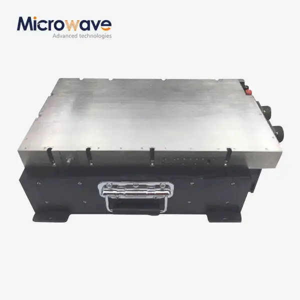 VIEW MOREAc Power Amplifier
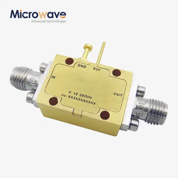 VIEW MOREVoltage Controlled Phase Shifter
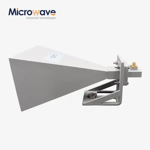 VIEW MOREStandard Horn Antenna
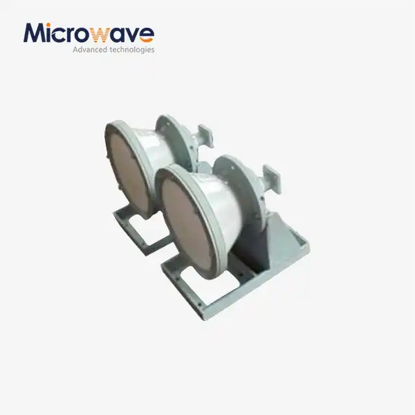 VIEW MOREConical Horn Lens Antenna
 VIEW MOREPoint Focusing Horn Lens Antenna
 VIEW MORECorrugated Horn and Multimode Horn Antenna
 VIEW MOREWideband Double-ridged Horn Antenna
 VIEW MOREMini Wideband Double-ridged Horn Antenna