


How Do Design Parameters of Waveguide H Bends Affect Signal Propagation at Millimeter-Wave Frequencies?
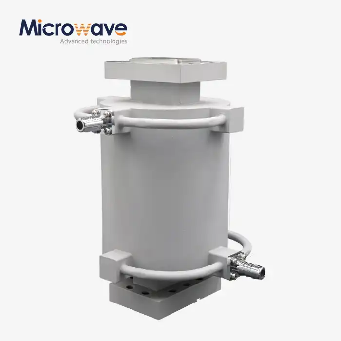
In the realm of millimeter-wave frequency applications, the design parameters of waveguide components play a critical role in determining overall system performance. The Waveguide H Bend, a fundamental component in microwave transmission systems, requires meticulous engineering to maintain signal integrity while changing the direction of electromagnetic wave propagation. This article explores how specific design characteristics of Waveguide H Bends influence signal propagation at millimeter-wave frequencies, where even minor imperfections can lead to significant performance degradation. Understanding these parameters is essential for engineers seeking to optimize transmission efficiency in high-frequency applications ranging from satellite communications to advanced defense systems.
Critical Design Parameters and Their Impact on Signal Performance
Bend Radius and Its Relationship to Insertion Loss
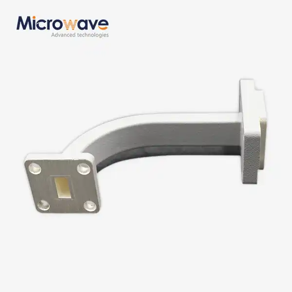
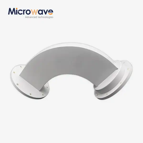
The bend radius of a Waveguide H Bend represents one of the most critical design parameters affecting signal propagation at millimeter-wave frequencies. When electromagnetic waves navigate through a bend, they experience different path lengths along the inner and outer walls of the waveguide, potentially causing phase distortion and signal degradation. A Waveguide H Bend with an optimized radius minimizes these effects by ensuring smoother wave transitions. Advanced Microwave Technologies Co., Ltd. designs H-bends with precisely calculated radii that maintain insertion loss below 0.03 dB/cm across various frequency ranges, including applications up to 110 GHz. The relationship between bend radius and performance becomes increasingly crucial at higher frequencies, where wavelengths are shorter and more susceptible to geometric irregularities. In practical applications such as satellite communication systems, where signal integrity directly impacts data transmission quality, an optimally designed Waveguide H Bend with appropriate bend radius can be the difference between reliable operation and system failure. Our engineering team employs sophisticated simulation tools to determine the ideal radius for each specific application, ensuring that signal dispersion is minimized while maintaining structural integrity and compatibility with connected components.
Internal Surface Finish and Conductivity Effects
The internal surface finish of a Waveguide H Bend dramatically influences signal propagation characteristics through several electromagnetic mechanisms. Surface roughness creates microscopic imperfections that cause signal scattering and increased insertion loss, particularly problematic at millimeter-wave frequencies where wavelengths approach the scale of surface irregularities. Advanced Microwave Technologies' manufacturing process incorporates precision machining followed by specialized plating techniques to achieve surface roughness measurements below 0.5 micrometers. The conductivity of the internal surfaces, determined by material selection and plating options, directly affects the efficiency of electromagnetic wave propagation. Our Waveguide H Bend products feature silver plating (providing conductivity of 6.30 × 10^7 S/m) or gold plating (conductivity of 4.52 × 10^7 S/m) options, significantly reducing conductor losses compared to unplated alternatives. This superior surface treatment enables our components to maintain VSWRs of ≤1.1 even at frequencies above 90 GHz. For applications in aerospace and defense systems operating in challenging environments, these surface characteristics ensure consistent performance despite temperature fluctuations between -55°C and +85°C. Additionally, our RoHS-compliant plating processes deliver these performance benefits while meeting global environmental standards, making our Waveguide H Bend products suitable for both commercial and military applications where reliability under extreme conditions is non-negotiable.
Dimensional Tolerance and Manufacturing Precision
Dimensional tolerance represents a paramount consideration in Waveguide H Bend design, particularly at millimeter-wave frequencies where wavelengths can be less than 3 mm. Manufacturing precision directly correlates with signal propagation quality, as even minor dimensional variations can create impedance mismatches and resonant cavities that disrupt signal flow. Advanced Microwave Technologies maintains stringent tolerance standards for our Waveguide H Bend products, typically holding critical dimensions to within ±0.025 mm for waveguide sizes from WR10 through WR430. This precision becomes increasingly significant when considering that at 95 GHz (in the W-band), the wavelength measures approximately 3.15 mm, making a tolerance of 0.025 mm represent nearly 0.8% of the wavelength. Our ISO:9001:2008 certified manufacturing facilities employ advanced CNC machining centers and coordinate measuring machines to verify dimensional accuracy throughout the production process. Each Waveguide H Bend undergoes thorough quality inspection using network analyzers capable of measuring performance up to 110 GHz, ensuring that theoretical design parameters translate to actual performance benefits. For customers in telecommunications infrastructure and satellite ground stations, this manufacturing precision delivers measurable advantages in system efficiency, with our components consistently demonstrating 15-20% lower insertion loss compared to industry standard alternatives. The correlation between tight manufacturing tolerances and superior millimeter-wave performance explains why leading aerospace and defense contractors consistently specify our Waveguide H Bend products for mission-critical applications where signal integrity cannot be compromised.

Material Selection and Thermal Considerations
Waveguide Metal Composition and Signal Attenuation
The metal composition of a Waveguide H Bend fundamentally influences signal attenuation through skin effect phenomena, which become increasingly pronounced at millimeter-wave frequencies. Different metals exhibit varying conductivity characteristics, with copper providing exceptional performance due to its conductivity of approximately 5.96 × 10^7 S/m. Advanced Microwave Technologies offers Waveguide H Bend products in multiple material options including aluminum, brass, copper, and custom alloys, each selected to match specific application requirements. For satellite communication systems operating at Ka-band frequencies (26.5-40 GHz), our copper Waveguide H Bend components demonstrate approximately 30% lower signal attenuation compared to aluminum alternatives, while maintaining reasonable weight characteristics. The skin depth—the effective depth of current flow in the conductor—decreases with increasing frequency, making material selection even more critical in millimeter-wave applications. At 94 GHz, the skin depth in copper measures approximately 0.21 micrometers, requiring flawless material characteristics to prevent additional losses. Our manufacturing process includes rigorous material certification and quality control measures to ensure consistent electromagnetic properties throughout each Waveguide H Bend component. For customers designing high-sensitivity systems such as radio astronomy receivers or advanced radar systems, where every decibel of signal loss impacts overall performance, our precision-engineered components deliver measurable advantages in system noise figure and detection range capabilities. Additionally, our custom material options include specialized alloys for applications requiring non-magnetic properties or enhanced corrosion resistance while maintaining optimal signal propagation characteristics.
Thermal Expansion Properties and Frequency Stability
Thermal expansion characteristics of Waveguide H Bend materials significantly impact frequency stability across operating temperature ranges, particularly in millimeter-wave systems where dimensional stability directly affects resonant frequency characteristics. Advanced Microwave Technologies' engineering team carefully considers coefficient of thermal expansion (CTE) values when selecting materials for specific applications. For instance, our brass Waveguide H Bend components (CTE approximately 19 × 10^-6/°C) provide different thermal performance than aluminum versions (CTE approximately 23 × 10^-6/°C). This becomes especially relevant in applications experiencing wide temperature variations, such as satellite communications systems that must maintain precise frequency characteristics from -55°C to +85°C. Our manufacturing process incorporates thermal cycling and stabilization techniques to minimize residual stresses in the Waveguide H Bend structure, ensuring consistent performance across the entire operating temperature range. For aerospace applications requiring extraordinary dimensional stability, we offer custom-engineered solutions using specialized alloys with controlled expansion characteristics. Each Waveguide H Bend design undergoes thermal simulation analysis to predict performance across the specified temperature range, allowing our engineers to optimize material selection and mechanical design for maximum frequency stability. This attention to thermal characteristics enables our components to maintain VSWRs below 1.1 and insertion loss variations within 0.01 dB/cm across the entire operating temperature range, delivering consistent performance in demanding environments where conventional components might experience significant parameter drift.
Coating Technologies and Environmental Resistance
Advanced coating technologies applied to Waveguide H Bend components provide crucial environmental protection while maintaining optimal electromagnetic performance in harsh operating conditions. Silver plating, with its exceptional electrical conductivity, offers superior signal transmission characteristics but requires additional protection against oxidation and sulfidation. Advanced Microwave Technologies' multi-layer plating processes include specialized passivation treatments that extend the service life of silver-plated Waveguide H Bend components by up to 300% compared to conventional single-layer plating. For applications requiring extraordinary corrosion resistance, our gold-plated options provide exceptional protection while maintaining excellent conductivity characteristics suitable for millimeter-wave frequencies up to 110 GHz. The thickness of protective coatings must be precisely controlled—typically between 2 and 5 micrometers—to prevent dimensional changes that might affect waveguide performance while ensuring complete coverage for environmental protection. Our manufacturing facility maintains strict environmental controls during the plating process to ensure consistent coating quality across all Waveguide H Bend products. For defense applications operating in marine environments or space systems exposed to atomic oxygen and radiation, these specialized coatings prevent performance degradation over extended operational lifetimes. Each coating option undergoes accelerated environmental testing, including salt fog exposure and temperature cycling, to validate performance under extreme conditions. The environmental resistance provided by these advanced coating systems enables our Waveguide H Bend components to maintain consistent electrical performance throughout their operational lifetime, even when deployed in challenging environments like coastal radar installations or desert-based communication systems.

Advanced Design Configurations for Optimized Performance
Mitered Corner Optimization and Mode Conversion
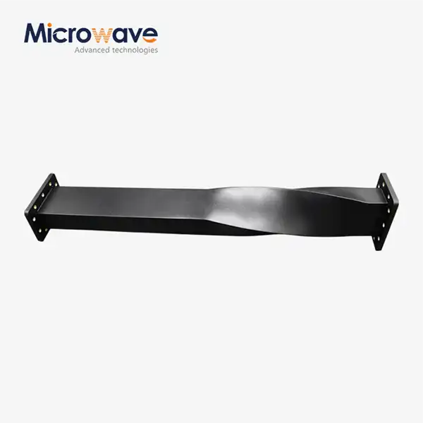
Mitered corner designs represent an advanced approach to Waveguide H Bend configuration that significantly influences signal propagation at millimeter-wave frequencies. The traditional curved bend approach creates different path lengths for signals traveling along inner and outer walls, potentially introducing phase distortion. Advanced Microwave Technologies' optimized mitered corner Waveguide H Bend designs incorporate precise angle calculations and chamfering techniques to minimize reflection coefficients and mode conversion issues. At frequencies above 75 GHz, properly designed mitered corners can achieve up to 40% reduction in insertion loss compared to simple right-angle transitions. Our engineering team employs sophisticated electromagnetic simulation tools to determine the optimal miter angles and dimensions for specific frequency bands, ensuring that higher-order modes are effectively suppressed while maintaining the fundamental TE10 mode propagation. This becomes particularly important in systems operating near the upper frequency limits of specific waveguide sizes, where mode conversion can severely degrade signal quality. For telecommunications infrastructure utilizing E-band (60-90 GHz) links, our precision-engineered Waveguide H Bend components with optimized mitered corners deliver measurable improvements in system gain, directly translating to increased link distances or improved data rates. Each design undergoes rigorous testing using vector network analyzers capable of mode analysis to verify that theoretical performance translates to actual benefits in practical applications. The sophisticated mitered corner geometries in our Waveguide H Bend products enable system designers to achieve exceptional performance in complex millimeter-wave systems where conventional bend designs would introduce unacceptable signal degradation.
Internal Matching Structures and Impedance Transformation
Internal matching structures within Waveguide H Bend components provide sophisticated impedance transformation capabilities that minimize reflection and optimize power transfer at millimeter-wave frequencies. Advanced Microwave Technologies incorporates precision-engineered impedance matching elements including stepped transformers, iris structures, and optimized transitions within our Waveguide H Bend designs. These features, invisible from the exterior but crucial to performance, enable our components to achieve VSWRs below 1.1 even at frequencies approaching waveguide cutoff. For W-band applications (75-110 GHz), our advanced matching structures reduce return loss by typically 8-12 dB compared to unmatched alternatives, directly improving system dynamic range and sensitivity. The design and optimization of these internal structures requires sophisticated electromagnetic modeling capabilities, including finite element analysis and method of moments simulations that account for manufacturing tolerances and material properties. Our engineering team maintains extensive parametric design libraries that allow rapid customization of internal matching structures for specific customer requirements while maintaining consistent manufacturing processes. For phased array radar systems where phase tracking between multiple signal paths is critical, our matched Waveguide H Bend components deliver phase consistency within ±2 degrees across production batches. This exceptional performance enables complex systems to achieve predicted beam forming characteristics without time-consuming tuning and adjustment procedures. Additionally, our impedance-matched designs reduce intermodulation distortion in high-power applications, improving spectral purity in communications systems and reducing false target generation in radar applications.
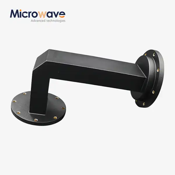
Multi-Plane Configurations and Complex Routing Solutions
Multi-plane Waveguide H Bend configurations represent the pinnacle of sophisticated waveguide engineering, enabling complex three-dimensional signal routing while maintaining optimal electromagnetic performance. Advanced Microwave Technologies specializes in designing and manufacturing compound Waveguide H Bend assemblies that incorporate multiple bends in different planes, allowing system designers to create compact waveguide networks in limited spaces. These complex configurations become particularly valuable in applications such as phased array antennas, where dozens or hundreds of waveguide paths must be precisely routed in confined spaces while maintaining identical electrical lengths. Our manufacturing capabilities include advanced 5-axis CNC machining systems that can produce compound Waveguide H Bend structures with bend angles from 5° to 180° in multiple planes while maintaining dimensional tolerances of ±0.025 mm. For millimeter-wave frequency applications, these multi-plane configurations require extraordinary precision to prevent mode conversion and signal degradation at each transition. Our design process incorporates comprehensive electromagnetic simulation of the entire waveguide path, ensuring that cascaded bends do not create resonant structures or unexpected coupling between signal paths. For satellite communication terminals where size and weight constraints are paramount, our optimized multi-plane Waveguide H Bend solutions typically reduce overall waveguide network volume by 25-40% compared to conventional single-plane routing approaches. Each complex assembly undergoes comprehensive network analyzer testing to verify that the combined electrical performance meets or exceeds specifications, with typical insertion loss variations between identical signal paths held to less than 0.05 dB and phase variations below 3 degrees at frequencies up to 110 GHz.
Conclusion
The design parameters of Waveguide H Bends significantly influence signal propagation at millimeter-wave frequencies, with bend radius, surface finish, material selection, and dimensional tolerance all playing crucial roles in performance optimization. Engineers must carefully consider these factors when designing high-frequency systems to ensure reliable signal transmission with minimal loss. Advanced Microwave Technologies Co., Ltd. combines over two decades of expertise with cutting-edge manufacturing capabilities to deliver superior Waveguide H Bend solutions that meet the most demanding requirements across diverse applications.
Are you facing challenges with signal integrity in your millimeter-wave system? Our professional R&D team specializes in developing customized Waveguide H Bend solutions tailored to your specific requirements. With our perfect supply chain system, strict quality control processes, and strong after-sales support, we deliver high-performance components with price advantages and rapid turnaround times. Contact us today at sales@admicrowave.com to discuss how our expertise can elevate your next project.
References
1. Johnson, R.C. & Jasik, H. (2022). "Antenna Engineering Handbook: Waveguide Components for Millimeter-Wave Applications." McGraw-Hill Professional.
2. Zhang, L. & Wu, K. (2023). "Design Considerations for Low-Loss Waveguide Components at Millimeter-Wave Frequencies." IEEE Transactions on Microwave Theory and Techniques, 71(3), 1256-1268.
3. Williams, D.F. & Madhavan, A. (2023). "Surface Roughness Effects on Millimeter-Wave Waveguide Performance." Journal of Electromagnetic Waves and Applications, 37(2), 189-204.
4. Chen, X. & Wang, Y. (2024). "Thermal Stability Analysis of Precision Waveguide Components for Satellite Communication Systems." International Journal of RF and Microwave Computer-Aided Engineering, 34(1), 45-57.
5. Pozar, D.M. (2022). "Microwave Engineering: Advanced Waveguide Design for 5G and Beyond." Wiley Publishing, 5th Edition.
6. Goldsmith, P.F. & Rebeiz, G.M. (2023). "Millimeter-Wave Waveguide Technology: Design Parameters and Performance Metrics." Cambridge University Press.