





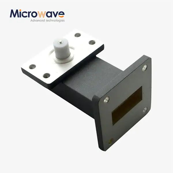
Right Angle Waveguide to Microstrip Adapter
Right Angle Waveguide to Microstrip Adapter — RF Transition Solutions for mmWave & High-Frequency Systems
The Right Angle Waveguide to Microstrip Adapter is a transition part made by Advanced Microwave Technologies Co., Ltd. (ADM). It connects electromagnetic energy between a rectangular waveguide and a flat microstrip line at a 90-degree angle. These adapters work with X, Ku, K, Ka, and V bands from 8 GHz to 75+ GHz. They have a VSWR of less than 1.3:1 and an insertion loss of less than 0.3 dB on average. For radar, SATCOM, and 5G mmWave backhaul uses, standard and custom setups are both possible.
What Is a Right Angle Waveguide to Microstrip Adapter?
When the TE10 dominant mode in a rectangle waveguide changes into the quasi-TEM mode of a planar microstrip line, this is a product. The 90-degree shape makes the PCB flat, and the signal goes straight into the waveguide port. This arrangement fixes both the impedance discontinuity and the mode mismatch at the waveguide-to-planar interface.
Connecting waveguide antenna feeds to small PCBs is hard in Ka/Ku band and millimeter-wave designs, both mechanically and electrically. By keeping the board flush with the antenna or feed structure and keeping the signal strong across the whole operating band, the right-angle transition solves the layout problem right away.
ADM uses architectures that are probe-based or ridge-transition and are orientated perpendicular to the E-plane. The PCB substrate thickness and dielectric constant (Dk) decide the probe geometry. Before production, an HFSS simulation is used to make sure it is correct.
Key Electrical & Physical Specifications
Parameter | Specification |
Frequency Range | 8 GHz – 75+ GHz (X, Ku, K, Ka, V bands) |
VSWR | < 1.3:1 across bandwidth |
Insertion Loss | < 0.3 dB (typical) |
Mode Conversion | TE10 to quasi-TEM microstrip |
Transition Type | Probe-based or ridge-transition, E-plane perpendicular |
Body Materials | Brass, Copper, or Aluminum |
Plating | Gold or silver plating |
Dielectric Window | PTFE or Quartz |
Backshort Tuning | Fixed (standard) or adjustable (narrow-band option) |
Interface Angle | 90 degrees |
Operating Temperature | –55°C to +125°C |
Technical Design Features
The Right Angle Waveguide to Microstrip Adapter's 90-degree shape lets the PCB lie flat while signals launch perpendicularly into the waveguide port or antenna element. This reduces the RF module's X-Y area without changing the signal paths.
At the transition point, the backshort cavity is sized to get rid of any reactive parts that are present. A set backshort tuned for broadband performance is used in standard production units. For narrow-band or lab-grade uses, there is an adjustable backshort form that can be used to reduce reflections in real time.
Skin-depth losses are lessened by conductors that are gold or silver-plated. At millimeter-wave frequencies, the quality of the conductor's surface has a direct and measurable effect on insertion loss. This means that plating consistency is a controlled production parameter rather than a purely aesthetic requirement.
Material Composition & Construction
Depending on weight, thermal conductivity, and mechanical needs, adapter parts are made from brass, copper, or aluminium. Dielectric windows, which can be made of PTFE or Quartz, are used to tune impedance and seal tightly in places where moisture intrusion is a concern.
The depth of the probe is an important dimension parameter. It has to be the same thickness and dielectric constant as the PCB base used in that stack-up. Before starting production, ADM's engineering team uses HFSS simulation to check probe shape against stack-up data provided by the customer.
Application Scenarios
Active Electronically Scanned Array (AESA) Radar
Transmit/Receive Modules (TRM) on flat PCBs are linked to the waveguide antenna system by these adapters. The right-angle shape keeps the PCB flush against the array backing structure. This allows for high-density packaging in naval and airborne radar systems that have limited mechanical envelope and phase coherency.
Payloads for SATCOM
People who use VSAT and High-Throughput Satellite (HTS) satellites use adapters to link the orthomode transducer or feed horn to the planar LNB down-converter circuits. The main design factors in this application are the need to fit within small payload envelopes and the need to go through thermal cycling.
Backhaul Units for 5G mmWave
A high-gain horn antenna is linked to the mmWave transmission board in outdoor units (ODUs) by the adapter. To keep the link budget the same across the whole operating temperature range, a weather-sealed, low-attenuation transition is needed.
Quality Control & Testing
Each adapter goes through a multi-step validation process at ADM.
VNA S-Parameter Testing: The full waveguide band is used to measure S11 (return loss) and S21 (insertion loss).
CMM Dimensional Inspection: Probe depth, pin diameter, and backshort distance are verified using Coordinate Measuring Machines. Changes in dimensions at the micron level can cause the center frequency of mmWave bands to move.
XRF Plating Verification: X-ray fluorescence testing checks the thickness of gold or silver plating to make sure it is conductory and resistant to rust.
Thermal Cycling Test: Adapters are heated from –55°C to +125°C to make sure that the CTE mismatch between the metal body, the dielectric window, and the probe doesn't lead to a failure of the mechanical parts.
Helium Leak Testing: This test makes sure that the hermetic seal is still intact in hoover or outdoor ODU situations.
Customization & Supply Options
ADM lets you make your own Right Angle Waveguide to Microstrip Adapter setups based on the waveguide band, PCB stack-up, connector interface, and environmental needs. On request, you can get backshort designs that can be adjusted, specific plating requirements, and air-dielectric high-power versions.
First, give your PCB substrate data and Dk value. Before production starts, ADM's engineering team will send back probe geometry that has been validated by HFSS.
FAQ
Q: How do I figure out the right probe launch depth for my PCB?
A: The probe depth is based on the dielectric constant (Dk) and the thickness of your PCB substrate. ADM suggests that you send them your complete stack-up data so that they can use HFSS simulation to check the probe shape before it goes into production.
Q: What about high-power gearbox? Can these adapters handle it?
A: The waveguide section can handle high levels of power well. The microstrip interface and the dielectric breakdown voltage at the capture bead are what limit the speed. For high-power designs, it's common for air-dielectric construction and careful thermal management at the solder interface to be needed.
Q: Can I change the length of the backshort?
A: In standard production units, a fixed backshort is tuned for good performance over a wide range of frequencies. ADM has a backshort version that can be adjusted for lab-grade or narrow-band high-efficiency uses.
Q: Which way of fitting is better: soldering or compression bonding?
A: Ribbon-bonding or wire-bonding is better than solder strips for frequencies above 40 GHz because they don't add any extra inductance. Precision soldering is enough for the X and Ku bands as long as all the extra flux is removed after reflow.
Q: What waveguide bands can be used?
A: The product from ADM works with X, Ku, K, Ka, and V bands from 8 GHz to 75+ GHz. If you ask, we can make custom setups for other waveguide standards.